
I´m trying to connect a DB25 to a 2A relay, the problem I have found it´s that I don´t know where at the ferduino code I can find the P00 value, and to what pin number (of the DB25) it´s connected to.
For example: PIN 1 from the relay 2 DB25 what´s correspond to? where could I assign a funtion to those pins at the code?
Thnak you very much in advance.
Forum ‹ Software ‹ Ferduino code ‹ Relay 2A pin config
can you send me a link to that program ? I translated a lot of the comments in my upscaled version but there's still a lot of it that needs done
Relay 2A pin config [SOLVED]
16 posts
• Page 1 of 1
Post Number:#1
 Tue Dec 09, 2014 5:13 pm
Posts: 10
Topics: 3 Solve rating: 0 Joined: Wed Oct 22, 2014 7:40 am Topics: 3
Age: 46 Gender: 
National Flag:

Post Number:#2
Tue Dec 09, 2014 5:37 pm


Posts: 1699
Topics: 38 Images: 301 Solve rating: 233 Joined: Mon Mar 03, 2014 5:59 pm Topics: 38
Age: 41 Location: São Paulo Gender: 
National Flag:

Have you checked this topic?
Basically you can connect anything to this pin.
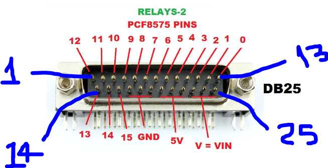
The pin 1 on DB25 is connected to P12 from PCF8575 as you can see here.
So, if you want control anything connected on P12 only use it on code:
Basically you can connect anything to this pin.
The pin 1 on DB25 is connected to P12 from PCF8575 as you can see here.
So, if you want control anything connected on P12 only use it on code:
Code: Select all
const byte MyDevice = 12;
Last edited by Fernando Garcia on Wed Dec 10, 2014 1:13 pm, edited 1 time in total.
Reason: Spelling.
Reason: Spelling.
Post your doubts on forum because it can help another user too. Just PM me for support if it's absolutely necessary.
Post Number:#3
Wed Dec 10, 2014 12:06 pm

Posts: 27
Images: 1 Solve rating: 1 Joined: Wed May 07, 2014 3:20 pm Age: 49 Gender: National Flag:

i have a problem too..
example:
if i want to connect heater on pin 1 of db25 and cooler on pin 2 of db25...
what should i change in the code?
if i write:
how could he know we are talking about pcf pin 1 and not normal pin 1?
example:
if i want to connect heater on pin 1 of db25 and cooler on pin 2 of db25...
what should i change in the code?
if i write:
Code: Select all
const byte heater = 1how could he know we are talking about pcf pin 1 and not normal pin 1?
Post Number:#4
Wed Dec 10, 2014 12:38 pm
Posts: 1699
Topics: 38 Images: 301 Solve rating: 233 Joined: Mon Mar 03, 2014 5:59 pm Topics: 38
Age: 41 Location: São Paulo Gender: National Flag:
Hi!
As I told above the pin 1 of DB25 is connected to P12 from PCF8575.
Maybe with this image stay more clear.
You need follow the logic used on topic quoted above.
Using names of variables available on Ferduino I'll give an example.
Only to keep the code organized.
Cut:
Paste after:
Change:
To an number following the order of free pins.
I'll use 0 (Zero) So.
On setup coment this line:
This function sets all pins from PCF8575 as OUTPUT, so the line above is useless.
In the tab "parametros" find all:
Replace all with:
This is the main difference between use a pin from Atmega and PCF8575.
So if you want control something connected to PCF8575 just add :
Before:
On this case I'm using the P0 from PCF8575 BUT this pin is available on pin 13 of DB25.
Let me know if is more clear now.
Best regards.
As I told above the pin 1 of DB25 is connected to P12 from PCF8575.
Maybe with this image stay more clear.
You need follow the logic used on topic quoted above.
Using names of variables available on Ferduino I'll give an example.
Only to keep the code organized.
Cut:
Code: Select all
const byte aquecedorPin = 42;Paste after:
Code: Select all
///**************** PCF8575 **********************************Change:
Code: Select all
const byte aquecedorPin = 42;To an number following the order of free pins.
I'll use 0 (Zero) So.
Code: Select all
const byte aquecedorPin = 0;On setup coment this line:
Code: Select all
pinMode(aquecedorPin, OUTPUT); This function sets all pins from PCF8575 as OUTPUT, so the line above is useless.
Code: Select all
  if(PCF8575TS_S == true)
   {
   PCF8575.begin(endereco_PCF8575TS); // Inicia a comunicação com o PCF8575TS
   for(int i = 0; i < 16; i++)
   {
   PCF8575.pinMode(i, OUTPUT);
   delay(100);
   PCF8575.digitalWrite(i, LOW);
   }
   }
In the tab "parametros" find all:
Code: Select all
digitalWrite(aquecedorPinReplace all with:
Code: Select all
PCF8575.digitalWrite(aquecedorPinThis is the main difference between use a pin from Atmega and PCF8575.
So if you want control something connected to PCF8575 just add :
Code: Select all
PCF8575.Before:
Code: Select all
digitalWriteOn this case I'm using the P0 from PCF8575 BUT this pin is available on pin 13 of DB25.
Let me know if is more clear now.
Best regards.
Post your doubts on forum because it can help another user too. Just PM me for support if it's absolutely necessary.
Post Number:#5
Wed Dec 10, 2014 3:39 pm
Posts: 27
Images: 1 Solve rating: 1 Joined: Wed May 07, 2014 3:20 pm Age: 49 Gender: National Flag:
Thank you Fernando, all clear now
Post Number:#6
Fri Dec 12, 2014 6:08 pm
Posts: 10
Topics: 3 Solve rating: 0 Joined: Wed Oct 22, 2014 7:40 am Topics: 3
Age: 46 Gender: National Flag:
Hi Fernando,
I have connected the PCF8575 using the parallel cable. I have launched the code test of PCF8575.
Measuring the output voltages with a voltimeter, taking pin 17 as GND, I have the follwing results:
- Pins 20, 21, 22 --> 5V That's Ok!
- Pins 1, 2, 3 --> Values ranging from 0v to 0.45v where they sholud be ranging from 0v to 5v. And this is the problem. Any idea of what is happening?
Edit: I have made the same test with the RJ45 relays and they work fine.
Post Number:#7
Fri Dec 12, 2014 7:12 pm
Posts: 1699
Topics: 38 Images: 301 Solve rating: 233 Joined: Mon Mar 03, 2014 5:59 pm Topics: 38
Age: 41 Location: São Paulo Gender: National Flag:
Hi!
It's normal because the PCF8575 is connected to two ULN2803 as explained here.
The signal is zero volt (GND). If you want 5V needs remove the ULN and do bridges as exaplined on topic above.
Best regards.
It's normal because the PCF8575 is connected to two ULN2803 as explained here.
The signal is zero volt (GND). If you want 5V needs remove the ULN and do bridges as exaplined on topic above.
Best regards.
Post your doubts on forum because it can help another user too. Just PM me for support if it's absolutely necessary.
Post Number:#8
Tue Dec 16, 2014 1:57 pm

Posts: 275
Topics: 6 Images: 46 Solve rating: 0 Joined: Mon Sep 08, 2014 1:35 am Topics: 6
Age: 44 Location: Byers Gender: National Flag:

Hi Fernando which tab do I add code for control of pins from PCF8575?
Happy reefing to all.
Christopher Kindig
Christopher Kindig
Post Number:#9
Tue Dec 16, 2014 2:42 pm
Posts: 1699
Topics: 38 Images: 301 Solve rating: 233 Joined: Mon Mar 03, 2014 5:59 pm Topics: 38
Age: 41 Location: São Paulo Gender: National Flag:
Have you checked this topic?
Post your doubts on forum because it can help another user too. Just PM me for support if it's absolutely necessary.
Post Number:#10
Tue Dec 16, 2014 2:44 pm
Posts: 27
Images: 1 Solve rating: 1 Joined: Wed May 07, 2014 3:20 pm Age: 49 Gender: National Flag:
On setup coment this line:
Select all
This function sets all pins from PCF8575 as OUTPUT, so the line above is useless.
In the tab "parametros" find all:
Select all
Replace all with:
Select all
Code: Select all
pinMode(aquecedorPin, OUTPUT);This function sets all pins from PCF8575 as OUTPUT, so the line above is useless.
Code: Select all
Code: Select all
  if(PCF8575TS_S == true)
   {
   PCF8575.begin(endereco_PCF8575TS); // Inicia a comunicação com o PCF8575TS
   for(int i = 0; i < 16; i++)
   {
   PCF8575.pinMode(i, OUTPUT);
   delay(100);
   PCF8575.digitalWrite(i, LOW);
   }
   }
In the tab "parametros" find all:
Select all
Code: Select all
digitalWrite(aquecedorPinReplace all with:
Code: Select all
PCF8575.digitalWrite(aquecedorPin
Post Number:#11
Tue Dec 16, 2014 3:15 pm
Posts: 275
Topics: 6 Images: 46 Solve rating: 0 Joined: Mon Sep 08, 2014 1:35 am Topics: 6
Age: 44 Location: Byers Gender: National Flag:
Yes I did those steps and now I need to where to put name for each pin for what it controls, like use pin 1 for heater , pin 2 for chiller ......
These for the most part are to the relay board, except the pi for chiller is going to need to be different as chiller has it's own relay built in, I am going to change it with a new one that use 5v trigger instead of 12v so ferduino can control with relay not turning power on and off.
These for the most part are to the relay board, except the pi for chiller is going to need to be different as chiller has it's own relay built in, I am going to change it with a new one that use 5v trigger instead of 12v so ferduino can control with relay not turning power on and off.
Happy reefing to all.
Christopher Kindig
Christopher Kindig
Post Number:#12
Tue Dec 16, 2014 4:35 pm
Posts: 1699
Topics: 38 Images: 301 Solve rating: 233 Joined: Mon Mar 03, 2014 5:59 pm Topics: 38
Age: 41 Location: São Paulo Gender: National Flag:
I don't know where's the problem, all information that I can give is related on this topic.
I just can say: I'm sorry for my bad english.
Maybe translating the comments in Ferduino tab can be more easy.
I just can say: I'm sorry for my bad english.
Maybe translating the comments in Ferduino tab can be more easy.
Code: Select all
const byte ledPinUV = 8; // Pin violet LEDs
const byte ledPinGreen = 9; // Pin green LEDs
const byte ledPinWhite = 10; // Pin white LEDs
const byte ledPinRoyBlue = 11; // Pin blue LEDs
const byte ledPinRed = 12; // Pin red LEDs
const byte fanPin = 13; // Pin that controls the fan speed Heatsink
// 14 & 15 pins reserved for serial port 3 that communicates with the "Stamps"
const byte multiplexadorS0Pin = 16; // Pin S0 control of stamps
const byte multiplexadorS1Pin = 17; // Pin S1 control of stamps
// 18 & 19 pins reserved for the RTC.
// 20 & 21 pins reserved for the PCF8575 I2C communication.
// Pins 22 ~ 41 reserved for LCD.
const byte aquecedorPin = 42; // Pin heater
const byte chillerPin = 43; // Pin chiller
const byte ledPinMoon = 44; // Pin moon light
const byte wavemaker1 = 45; // Pin wavemaker 1
const byte wavemaker2 = 46; // Pin wavemaker 2
const byte ozonizadorPin = 47; // Pin ozone
const byte reatorPin = 48; // Pin calcium reactor
Last edited by Fernando Garcia on Fri Jan 16, 2015 8:45 am, edited 1 time in total.
Reason: Spelling.
Reason: Spelling.
Post your doubts on forum because it can help another user too. Just PM me for support if it's absolutely necessary.
Post Number:#13
Tue Dec 16, 2014 7:32 pm
Posts: 275
Topics: 6 Images: 46 Solve rating: 0 Joined: Mon Sep 08, 2014 1:35 am Topics: 6
Age: 44 Location: Byers Gender: National Flag:
ok I see all are named in ferduino tab thank you fernando.
Happy reefing to all.
Christopher Kindig
Christopher Kindig
Post Number:#14
Wed Dec 17, 2014 3:22 am
Posts: 275
Topics: 6 Images: 46 Solve rating: 0 Joined: Mon Sep 08, 2014 1:35 am Topics: 6
Age: 44 Location: Byers Gender: National Flag:
I found program that will translate all the comments without missing with the code one done would you like I can send it back and you can use as english.
Happy reefing to all.
Christopher Kindig
Christopher Kindig
Post Number:#15
Thu Dec 18, 2014 1:23 am


Posts: 68
Topics: 2 Solve rating: 0 Joined: Thu Apr 10, 2014 7:59 pm Topics: 2
Age: 59 Location: Barbourville, Kentucky Gender: National Flag:
I found program that will translate all the comments without missing with the code one done would you like I can send it back and you can use as english.
can you send me a link to that program ?
I translated a lot of the comments in my upscaled version but there's still a lot of it that needs done
Post Number:#16
Thu Dec 18, 2014 3:00 am
Posts: 275
Topics: 6 Images: 46 Solve rating: 0 Joined: Mon Sep 08, 2014 1:35 am Topics: 6
Age: 44 Location: Byers Gender: National Flag:
Sorry willy the program won't what I thought, I have to do one tab at a time 
-------------------------------- Last edited Thu Dec 18, 2014 12:08 am --------------------------------
Sorry willy the program won't what I thought, I have to do one tab at a time
-------------------------------- Last edited Thu Dec 18, 2014 12:08 am --------------------------------
Sorry willy the program won't what I thought, I have to do one tab at a time
-------------------------------- Last edited Thu Dec 18, 2014 12:08 am --------------------------------
Sorry willy the program won't what I thought, I have to do one tab at a time
-------------------------------- Last edited Thu Dec 18, 2014 12:08 am --------------------------------
Sorry willy the program won't what I thought, I have to do one tab at a time
Happy reefing to all.
Christopher Kindig
Christopher Kindig
16 posts
• Page 1 of 1
Who is online
Users viewing this topic: No registered users and 1 guest